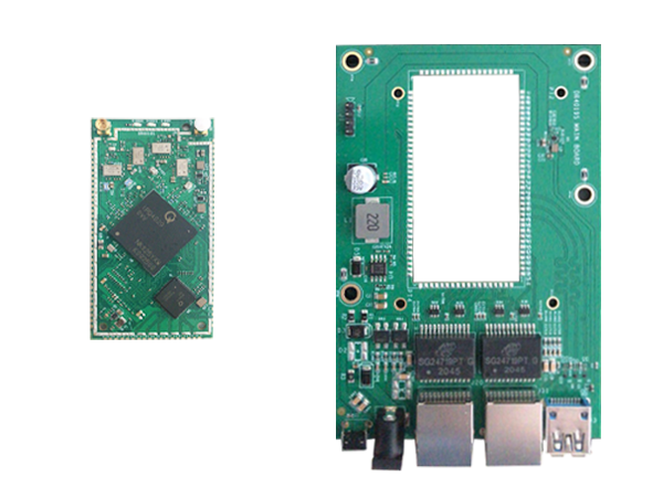
Featuring withindustrial-grade IPQ4019 chipset
Integrated with 2x 2 5G high power
Radio module and 2x2 2.4G high power Radio module
Support 5.180GHz to5.825GHz Frequency Range;
Support 2.412GHz to 2.482GHz
Support 2 x 5G MMCX Connectors and 2x2.4G MMCX
20MHz/40MHz/80MHz Bandwidth
Support 11ABGN/802.11AC
RoHS compliance ensure a high level
protection of human health and the environment from risks that can be posed by
Support Openwifi
Support QSDK
Support Openwrt

| Absolute Maximum Rating |
Parameter | Rating | Unit |
Supply Voltage | 24V~48 | V |
Operating Temperature Range | -40 to +70 | ºC |
Storage Temperature Range | -45 to +105 | ºC |
Operating Humidity Range | 5 to +95 (non-condensing) | % |
Storage Humidity Range | 0 to +90 (non-condensing) | % |
Hardware Specifications |
Symbol | Parameter |
CPU | IPQ4019(Quad core ARM Cortex A7 at 716.8 MHz) |
Antenna Connector | 2 x 5G MMCX connectors;2x2.4G MMCX |
10/100/1000Mbps |
2xRJ45 |
DC Jack | 12 power supply |
ROHS Compliance | YES |
Dimension | 65mmx35mm x 16mm |
Max Power | 12V x 0.8A= 9.6W |
Nor Flash | 32MB |
DDR | 256MB |
Radio TX Specifications(5180MHz-5825MHz) |
Operating Mode | Data Rate | Power | Tolerance | |
1 Chain | 2 Chains | |||
802.11a | 6 Mbps | 26dBm | 29dbm | ±2dB |
54 Mbps | 22dBm | 25dbm | ±2dB | |
802.11n HT20 | MCS0, MCS8 | 26dBm | 29dbm | ±2dB |
MCS7, MCS15 | 22dBm | 25dbm | ±2dB | |
802.11n HT40 | MCS0, MCS8 | 25dBm | 28dbm | ±2dB |
MCS7, MCS15 | 21dBm | 24dbm | ±2dB | |
802.11ac | MCS0, MCS10,MCS20 | 25dBm | 28dbm | ±2dB |
MCS9,MCS19,MCS29 | 19dBm | 22dbm | ±2dB | |
Radio RX Specifications(5180MHz-5825MHz) |
Operating Mode |
Data Rate |
Sensitivity |
802.11a
| 6 Mbps | -92dBm |
54 Mbps | -74dBm | |
802.11n HT20
| MCS0, MCS8 | -91dBm |
MCS7, MCS15 | -72dBm | |
802.11n HT40
| MCS0, MCS8 | -90dBm |
MCS7, MCS15 | -70dBm | |
802.11AC HT40
| MCS0, MCS10,MCS20 | -90dBm |
MCS9,MCS19,MCS29 | -67dBm | |
802.11AC HT80
| MCS0, MCS10,MCS20 | -88dBm |
MCS9,MCS19,MCS29 | -62dBm |
Radio TX Specifications(2412MHz-2482MHz) |
Operating Mode
| Data Rate
| Power | Tolerance
| |
1 Chain | 2 Chains | |||
802.11g
| 6 Mbps | 25dbm | 28dbm | ±2dB |
54 Mbps | 22dbm | 25dbm | ±2dB | |
802.11n HT20
| MCS0, MCS8 | 25dbm | 28dbm | ±2dB |
MCS7, MCS15 | 21dbm | 24dbm | ±2dB | |
802.11n HT40
| MCS0, MCS8 | 25dbm | 28dbm | ±2dB |
MCS7, MCS15 | 21dbm | 24dbm | ±2dB | |
Radio RX Specifications(2412MHz-2482MHz) |
Operating Mode |
Data Rate |
Sensitivity |
802.11g
| 6 Mbps | -91dBm |
54 Mbps | -73dBm | |
802.11n HT20
| MCS0, MCS8 | -90dBm |
MCS7, MCS15 | -72dBm | |
802.11n HT40
| MCS0, MCS8 | -90dBm |
MCS7, MCS15 | -70dBm |
| Pin Define |

Pin number | signal | Pin number | signal | Pin number | signal |
1 | GND | 36 | GND | 54 | GND |
2 | GND | 37 | GND | 55 | P4_TRX2+ |
3 | GND | 38 | GND | 56 | P4_TRX2- |
4 | GND | 39 | GND | 57 | P4_TRX3+ |
5 | GND | 40 | GND | 58 | P4_TRX3- |
6 | GND | 41 | P3_TRX0+ | 59 | GND |
7 | GND | 42 | P3_TRX0- | 60 | P4_1000_LED |
8 | GND | 43 | P3_TRX1+ | 61 | 2G_LINK_LED_1P8 |
9 | GND | 44 | P3_TRX1- | 62 | GND |
10 | GND | 45 | P3_TRX2+ | 63 | GND |
11 | GND | 46 | P3_TRX2- | 64 | USB3_SS_TX_P |
12 | GND | 47 | P3_TRX3+ | 65 | USB3_SS_TX_N |
13 | GND | 48 | P3_TRX3- | 66 | USB3_SS_RX_P |
14 | GND | 49 | P4_TRX0+ | 67 | USB3_SS_RX_N |
15 | GND | 50 | P4_TRX0- | 68 | USB3_HS_DP |
16 | GND | 51 | P4_TRX1+ | 69 | USB3_HS_DM |
17 | GND | 52 | P4_TRX1- | 70 | GND |
18 | GND | 53 | GND | 71 | 2G_STRENGTH_LED |
19 | GND |
|
| 72 | GND |
20 | GND |
|
| 73 | GND |
21 | GND |
|
| 74 | GND |
22 | GND |
|
| 75 | GND |
23 | GND |
|
| 76 | GND |
24 | GND |
|
| 77 | GND |
25 | GND |
|
| 78 | GND |
26 | GND |
|
| 79 | 12V |
27 | GND |
|
| 80 | 12V |
28 | GND |
|
| 81 | GND |
29 | GND |
|
| 82 | GND |
30 | software reset |
|
| 83 | GND |
31 | GND |
|
| 84 | GND |
32 | 3.3V |
|
| 85 | GND |
33 | Uart TX |
|
| 86 | GND |
34 | Uart RX |
|
| 87 | GND |
35 | GND |
|
| 88 | GND |
Note:
1) Pin41-Pin48 indicates the differential signals of network port 1, which are 0,1,2, and 3 in sequence
2) Pin48 to Pin52, P55 to Pin58 indicates the differential signals of network port 2. The sequence is differential signals 0,1,2, and 3
The schematic diagram of the extended circuit is as follows:

3) Pin64-Pin69 indicates the differential signals of USB3.0 are TX, RX, and HS in sequence
The schematic diagram of the extended circuit is as follows:

4) Pin 79,80 is a 12V input power signal and the input voltage is in the range of 11v-13v
5) Pin32 -Pin35 indicates the serial port signal, Pin32 indicates the output 3.3V, Pin33, and Pin34 indicates the output input signal
The schematic diagram of the extended circuit is as follows,

ADD:116 ChengYang Road, XiangCheng District, SuZhou City,JiangSu Province, China
Teams:544199036@qq.com
Email:support@wallystech.com


Copyright © 2020 Wallys Communications (Suzhou ) Co., LTD Sitemap